Author Affiliations
Abstract
1 State Key Laboratory of Integrated Optoelectronics, College of Electronic Science and Engineering, Jilin University, Changchun 130012, China
2 College of Communication Engineering, Jilin University, Changchun 130012, China
3 State Key Laboratory of Supramolecular Structure and Materials, Institute of Theoretical Chemistry, Jilin University, Changchun 130012, China
4 College of Information Technology, Jilin Agricultural University, Changchun 130118, China
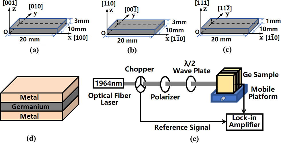
In this Letter, we have demonstrated significant electric field induced (EFI) optical rectification (OR) effects existing in the surface layers of germanium (Ge) and measured the distributions of EFI OR signals along the normal directions of surface layers of Ge samples. Based on the experimental results, the ratios of the two effective second-order susceptibility components χzzz(2eff)/χzxx(2eff) for Ge(001), Ge(110), and Ge(111) surface layers can be estimated to be about 0.92, 0.91, and 1.07, respectively. The results indicate that the EFI OR can be used for analyzing the properties on surface layers of Ge, which has potential applications in Ge photonics and optoelectronics.
240.4350 Nonlinear optics at surfaces 190.4350 Nonlinear optics at surfaces Chinese Optics Letters
2018, 16(10): 102401

Author Affiliations
Abstract
1 State Key Laboratory on Integrated Optoelectronics, College of Electronic Science and Engineering, Jilin University, Changchun 130012, China
2 College of Communication Engineering, Jilin University, Changchun 130012, China
3 College of Information Technology, Jilin Agricultural University, Changchun 130118, China
4 State Key Laboratory on Integrated Optoelectronics, Institute of Semiconductors, Chinese Academy of Sciences, Beijing 100083, China
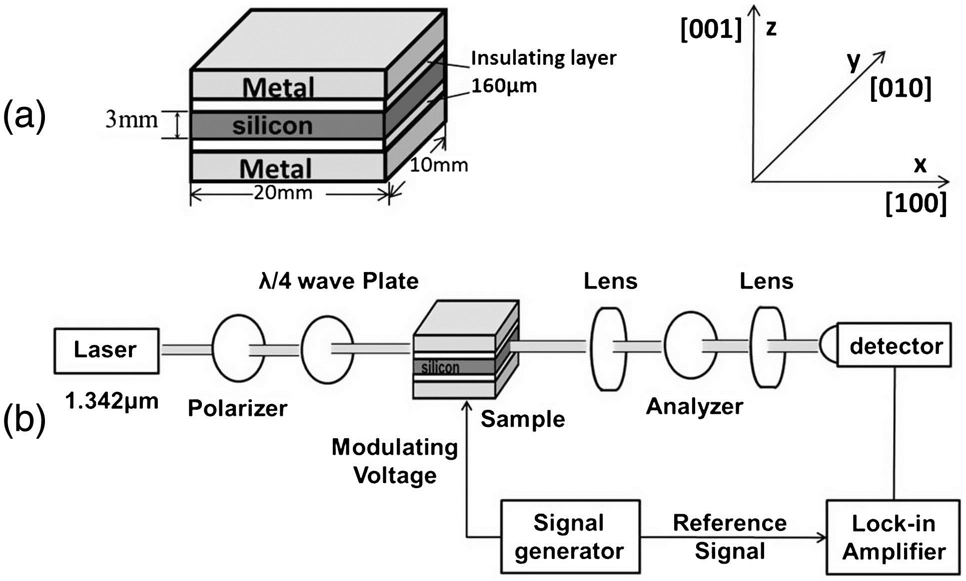
The depth profile of electric-field-induced (EFI) optical rectification (OR) and EFI Pockels effect (PE) in a Si(110) crystal are investigated. The results show that EFI OR and PE signals are very sensitive to the electric field strength in the surface layers of the Si crystal. Theoretical formulas that include the electric field parameters and the widths of the space-charge region are presented and agreed very well with the experimental results. The experiments and simulations indicate that EFI OR and PE are potential methods for researching the surface/interface properties along the depth direction in centrosymmetric crystals such as Si.
240.4350 Nonlinear optics at surfaces 190.4350 Nonlinear optics at surfaces 190.4720 Optical nonlinearities of condensed matter Chinese Optics Letters
2017, 15(6): 062401
Author Affiliations
Abstract
1 State Key Laboratory on Integrated Optoelectronics, College of Electronic Science and Engineering, Jilin University, Changchun 130012, China
2 College of Communication Engineering, Jilin University, Changchun 130012, China
3 College of Information Technology, Jilin Agricultural University, Changchun 130118, China
4 Changchun Institute of Applied Chemistry, Chinese Academy of Sciences, Changchun 130022, China
Pockel’s effect and optical rectification induced by the built-in electric field in the space charge region of a silicon surface layer are demonstrated in a {001}-cut high-resistance silicon crystal. The half-wave voltage is about 203 V, deduced by Pockel’s effect. The ratio χzxx(2)/χzzz(2) is calculated to be about 0.942 according to optical rectification. Our comparison with the Kerr signal shows that Pockel’s signal is much stronger. This indicates that these effects are so considerable that they should be taken into account when designing silicon-based photonic devices.
230.2090 Electro-optical devices 190.4350 Nonlinear optics at surfaces Chinese Optics Letters
2016, 14(1): 012301
Author Affiliations
Abstract
The nonlinear photoresponse to a 1.56-\mu m infrared continuous wave laser in semi-insulating (SI) galliumarsenide (GaAs) is examined. The double-frequency absorption (DFA) is responsible for the nonlinear photoresponse based on the quadratic dependence of the photocurrent separately on the coupled optical power and bias voltage. The electric field-induced DFA remarkably affects the native DFA in SI GaAs. The surface electric field or the surface band-bending of SI GaAs significantly affects the magnitude variation of the photocurrent and dark current.
250.4390 Nonlinear optics, integrated optics 250.0040 Detectors 190.4400 Nonlinear optics, materials 190.4350 Nonlinear optics at surfaces Chinese Optics Letters
2013, 11(11): 112501
1 吉林大学 通信工程学院 光通信系,吉林 长春 130012
2 集成光电子学国家重点实验室吉林大学实验区,吉林 长春 130012
3 吉林大学 电子科学与工程学院,吉林 长春 130012
以沿[110]晶向切割的近本征硅单晶为样品,通过研究样品对连续波固体激光器所产生的1.3 μm的近红外光的双光子吸收所诱导的光电流对入射光偏振方向的依赖关系,研究了双光子吸收的各向异性.测得了硅单晶对该波长的光的三阶极化率张量χ(3)的各向异性系数为-0.25,两个独立分量的比值χxxxx/χxxyy的幅度为2.4,并基于前期工作所得的χxxyy的结果,进而确定了另一分量χxxxx的值大约为1.49×10-19 m2/V2.
非线性光学 硅单晶 双光子吸收 三阶极化率 非线性各向异性 nonlinear optics silicon crystal two-photon absorption third-order susceptibility nonlinear anisotropy
Author Affiliations
Abstract
Different electro-optic effects, such as Kerr effect, Pockels effect induced by the electric field or strain, and plasma dispersion effect exist in silicon. Experimentally distinguishing these effects is necessary for designing silicon-based electro-optic devices. According to their different polarization dependencies and frequency responses, these effects are measured and distinguished successfully via a transverse electro-optic modulation experiment based on the near-intrinsic silicon sample. The results indicate that Pockels effect induced by the electric field or strain is primary among these effects in the near-intrinsic silicon sample.
230.2090 Electro-optical devices 190.3270 Kerr effect 260.1440 Birefringence Chinese Optics Letters
2012, 10(8): 082301
Author Affiliations
Abstract
The transverse electro-optic (EO) modulation system is built based on cubic boron nitride (cBN) single crystals unintentionally doped and synthesized at a high pressure and high temperature. The photoelectric output of the system includes two parts that can be measured respectively and the value of elements in the linear EO tensor of the cBN crystal can be obtained. This method does not need to measure the absolute light intensity. All of the surfaces of the tiny cBN crystals whose hardness is next to the hardest diamonds are {111} planes. The rectangular parallelepiped cBN samples are obtained by cleaving along {110} planes and subsequently grinding and polishing f112g planes of the tiny octahedral cBN flakes. Three identical non-zero elements of the EO tensor of the cBN crystal are measured via two sample configurations, and the measured results are very close, about 3.68 and 3.95 pm/V, respectively, which are larger than the linear EO coefficients of the general III-V compounds.
160.2100 Electro-optical materials 160.4760 Optical properties 190.4400 Nonlinear optics, materials 190.4720 Optical nonlinearities of condensed matter Chinese Optics Letters
2012, 10(4): 041602
1 吉林大学电子科学与工程学院, 集成光电子学国家重点实验室, 吉林 长春
2 黑龙江大学电子工程学院, 黑龙江 哈尔滨 850010
3 长春理工大学光电信息技术学院, 吉林 长春 130012
对于微小尺寸的N型宽禁带立方氮化硼(CBN)半导体晶体, 在施加恒稳电场的情况下, 观察到电致发光现象。 通过置CBN单晶样品于光栅单色仪抛物面反射镜焦点的方法, 对于CBN的蓝紫光辐射获得了测试系统的最大入射光通量和理想的信噪比。 在350~450 nm波长范围内, CBN加上4.7×10⁶ V?cm-1恒稳电场条件下, 测量出立方氮化硼的蓝紫光发射光谱。同时, 结合基于第一性原理的GGA方法计算出的立方氮化硼能带结构和电子态密度, 以及测量得到的非线性j-E关系和电击穿特性, 讨论了发光机理。 提出了在雪崩击穿前的缺陷偶极子极化和击穿后, 产生大量的激发态电子, 电子在Γ能谷和X能谷间迁移的发光机制。Cubic Boron Nitride Crystal
立方氮化硼单晶 蓝紫光辐射 能谷 梯度矫正局域密度近似(GGA) Cubic boron nitride crystal Blue-violet light-emitting Energy
Author Affiliations
Abstract
1 State Key Laboratory on Integrated Optoelectronics, College of Electronic Science and Engineering, Jilin University, Changchun 130012, China
2 College of Communication Engineering, Jilin University, Changchun 130012, China
3 Applied Technique College, Jilin University, Changchun 130012, China
4
5 State Key Laboratory on Integrated Optoelectronics, College of Electronic Science and Engineering, Jilin University, Changchun 130012, China:
Diamonds are wide-gap semiconductors possessing excellent physical and chemical properties; thus, they are regarded as very appropriate materials for optoelectronic devices. Based on the Kerr effect, we introduce a simple and feasible method for measuring the third-order nonlinear optical susceptibility of synthetic diamonds. In the experiments, synthetic type I diamond samples and transverse electro-optic modulation systems are utilized. As for the laser with the wavelength of 650 nm, the third-order susceptibility and Kerr coefficient of the diamond samples are obtained at χ(3)1212=2:17×10-23 m2=V2 and S44= 1.93×10⁻²³ m2=V2, respectively.
合成金刚石 克尔效应 三阶非线性光学极化率 160.4670 Optical materials 190.3270 Kerr effect 160.4760 Optical properties Chinese Optics Letters
2010, 8(7): 685
集成光电子学国家重点联合实验室吉林大学电子科学与工程学院, 吉林 长春 130012
从经典的极化理论出发, 分析了直流电场、低频调制电场和光波电场共同存在时硅材料折射率的变化, 从理论上揭示了场致线性电光效应的物理实质。以近本征硅材料为样品, 采用金属-绝缘体-半导体样品结构, 搭建了由塞纳蒙(Senarmont)补偿器改进成的横向电光调制系统。在硅材料空间电荷区内观测到显著的线性电光调制效应, 系统的半波电压小于170 V, 从实验上直接证实了硅材料中内建电场诱导的场致线性电光效应的存在。此外还观测到由克尔效应引起的二次电光调制信号, 以及由场致光整流效应引起的、随线偏振光的方位角的二倍余弦变化的电信号。实验结果与经典极化理论的预期完全一致, 也间接证实了硅材料中场致线性电光效应的存在。
非线性光学 场致线性电光效应 场致光整流 克尔效应 横向电光调制 硅材料


